

In this article we will look at 8051 microcontroller, its pin diagram and architecture along with different components.
Watch this video for introduction to microcontrollers:
Contents
Introduction to 8051 Microcontroller
The Intel 8051 microcontroller is one of the most popular general purpose microcontrollers in use today. The success of the Intel 8051 spawned a number of clones, which are collectively referred to as the MCS-51 family of microcontrollers, which includes chips from vendors such as Atmel, Philips, Infineon, and Texas Instruments.
Watch this video to learn about 8051 microcontroller and instruction set:
The Intel 8051 is an 8-bit microcontroller which means that most available operations are limited to 8 bits. Some of the features that have made the 8051 popular are:
- 4 KB on chip program memory
- 128 bytes on chip data memory (RAM)
- 4 register banks
- 128 user defined software flags
- 8-bit data bus
- 16-bit address bus
- 16-bit timers (usually 2, but may have more, or less)
- 3 internal and 2 external interrupts
- Bit as well as byte addressable RAM area of 16 bytes
- 16-bit program counter and data pointer
8051 Schematic Diagram
8051 Schematic Diagram is as shown in the below figure.
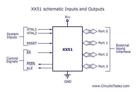
We can see 3 system inputs, 3 control signals and 4 ports (for external interfacing). A Vcc power supply and ground is also shown. System inputs are necessary to make the micro controller functional. So the first and most important of this is power, marked as Vcc with a GND (ground potential). XTAL 1 and XTAL 2 are for the system clock inputs from crystal clock circuit.
RESET input is required to initialize microcontroller to default/desired values and to make a new start. There are 3 control signals EA, PSEN and ALE. These signals known as External Access (EA), Program Store Enable (PSEN), and Address Latch Enable (ALE) are used for external memory interfacing. There are four ports numbered 0,1,2,3 and called as Port 0, Port 1, Port 2 and Port 3 which are used for external interfacing of devices like DAC, ADC, 7 segment display, LED etc. Each port has 8 I/O lines and they all are bit programmable.
8051 Pin Diagram
8051 Pin Diagram is as shown in the figure below.
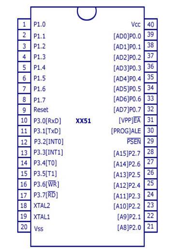
Pins 1-8
- Known as Port 1. Unlike other ports, this port does not serve any other functions
- Port 1 is an internally pulled up, quasi bi directional I/O port
Pin 9
- As explained before RESET pin is used to set the 8051 microcontroller to its initial values, while the microcontroller is working or at the initial start of application
- The RESET pin must be set high for 2 machine cycles
Pins 10-17
- Known as Port 3
- This port also serves some other functions like interrupts, timer input, control signals for external memory interfacing RD and WR , serial communication signals RxD and TxD etc
- This is a quasi bi directional port with internal pull up
Pins 18 and 19
- Used for interfacing an external crystal to provide system clock
Pin 20
- Named as Vss – it represents ground (0 V) connection
Pins 21-28
- Known as Port 2 (P 2.0 to P 2.7) – in addition to serving as I/O port, higher order address bus signals are multiplexed with this quasi bi directional port
Pin 29
- PSEN or Program Store Enable is used to read signal from external program memory
Pin 30
- ALE aka Address Latch Enable is used to demultiplex the address-data signal of port 0 (for external memory interfacing)
- 2 ALE pulses are available for each machine cycle
Pin 31
- EA/ External Access input is used to enable or disallow external memory interfacing
- If there is no external memory requirement, this pin is pulled high by connecting it to Vcc
Pins 32-39
- Known as Port 0 (P0.0 to P0.7) – In addition to serving as I/O port, lower order address and data bus signals are multiplexed with this port (to serve the purpose of external memory interfacing)
- This is a bi directional I/O port (the only one in 8051) and external pull up resistors are required to function this port as I/O
Pin 40
- Named as Vcc is the main power source
- Usually its +5V DC
8051 Architecture
The simplified internal architecture of 8051 is as illustrated below.
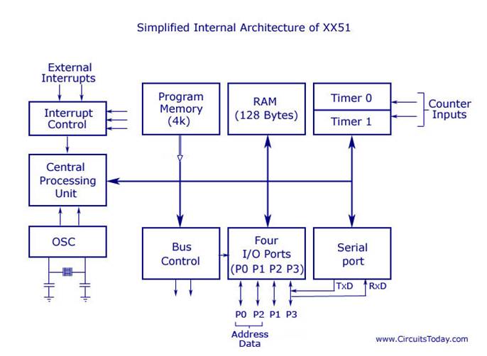
The system bus connects all the support devices with the central processing unit. 8051 system bus composes of an 8 bit data bus and a 16 bit address bus and bus control signals. RxD and TxD (serial port input and output) are interfaced with port 3.
8051 Instruction Set
The complete 8051 Instruction Set or all 8051 instructions are broadly classified in to four groups:
- Data moving/handling instructions
- Logical instructions
- Arithmetic instructions
- Branching instructions
Some examples of data moving/handling instructions are as shown in the table below.
| Mnemonics | Description | Addressing Mode | No.of Bytes Occupied | No.of Cycles Used |
| Mov a, #num | Copy the immediate data num into acc | Immediate | 2 | 1 |
| Mov Rx, a | Copy the data from acc to Rx | Register | 1 | 1 |
| Mov a, add | Copy the data from direct address add to acc | Direct | 2 | 1 |
| Mov a, @Rp | Copy the data that is at address in Rp to acc | Indirect | 2 | 2 |
Some examples of logical instructions are as shown in the table below.
| Mnemonics | Description | Addressing Mode | No.of Bytes Occupied | No.of Cycles Used |
| Clr a | Clear each bit of acc | Direct | 1 | 1 |
| Cpl a | Complement each bit of acc | Direct | 1 | 1 |
| Rl a | Rotate acc one bit left | – | 1 | 1 |
| Rr a | Rotate acc one bit right | – | 1 | 1 |
Some examples of arithmetic instructions are as shown in the table below.
| Mnemonics | Description | Addressing Mode | No.of Bytes Occupied | No.of Cycles Used |
| Inc a | Add 1 to acc | Register | 1 | 1 |
| Inc add | Add 1 to the content of add | Direct | 2 | 1 |
| Addc a, #num | Add the immediate num with acc and carry, stores result in acc | Immediate | 2 | 1 |
| Dec a | Subtract 1 from acc | Register | 1 | 1 |
Some examples of branching instructions are as shown in the table below.
| Mnemonics | Description | No.of Bytes Occupied | No.of Cycles Used |
| Jc label | Jump to label if carry is set to 1 | 2 | 2 |
| Jnc label | Jump to label if carry is cleared to 0 | 2 | 2 |
| Jz label | Jump to label if content of acc is 0 | 2 | 2 |
| Nop | Short form of no operation means do nothing and go to next instruction | 1 | 1 |

Suryateja Pericherla, at present is a Research Scholar (full-time Ph.D.) in the Dept. of Computer Science & Systems Engineering at Andhra University, Visakhapatnam. Previously worked as an Associate Professor in the Dept. of CSE at Vishnu Institute of Technology, India.
He has 11+ years of teaching experience and is an individual researcher whose research interests are Cloud Computing, Internet of Things, Computer Security, Network Security and Blockchain.
He is a member of professional societies like IEEE, ACM, CSI and ISCA. He published several research papers which are indexed by SCIE, WoS, Scopus, Springer and others.
Leave a Reply